This article discusses clock configuration, prescalers, and GPIO clock output, facilitating understanding of ARM processors.
Introduction
The ARM clock scheme is a very complex; but, flexible system allowing the developer to control various sections of the processor using a collection of: clock sources, clock multiplexers and prescalers propagating the signal along a series of buses to the various peripherals.
With most other processors, the system clock is continuously active; but in the ARM ecosystem, each clock can be independently switched on and off to conserve power. In this way, peripherals that are not being used are not clocked and therefore not drawing valuable resources.
The example code and this article's discussion will center around an STM32 NUCLEO-64 board featuring the STM32F411RE processor. The board is manufactured by STMicroelectonics and is a 32-bit Cortex-M4 MCU. The ARM family of processors provide solutions in a wide range of areas that address performance, power and cost requirements.
The STM32F411RE processor is a 32bit Cortex-M4 microcontroller with a maximum clock speed of 100MHz that requires a 1.7V to 3.6V supply, contains 512KB flash and 128KB SRAM. Peripherals include 81 I/O ports, of which 77 are 5V tolerant, 3 I2C interfaces, 3 USARTS, 5 SPI, an OTG USB, 16 channels ADC, 11 Timers, DMA and CRC.
Be aware that while the power supplied to the device is 3.3V some pins are 5V tolerant. Refer to the STM32F411RE datasheet in the section "Pinouts and pin description" for details. This is pertinent only when the pin is configured as input, when configured as output the pin outputs at the 3.3V level.
I am in no way affiliated with or receive any compensation from STMicroelectronis, I only chose this family of devices because they were inexpensive, the IDE was free, with no restrictions, and I'm a cheap bastard.
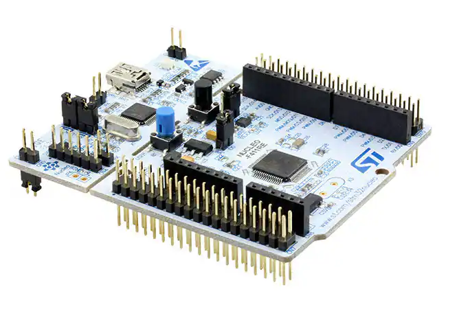
Figure 1: NUCLEO-64 featuring the STM32F411RE processor
To follow along with the code examples, you will need the items listed in the following table. Any ARM processor in the M4 family should work for these examples but the examples provided were written and tested on the NUCLEO-64 board that has an STM32F411RE processor. The board has an ST-LINK programmer/debugger on board so it can be used directly from the STM32CubeIDE. (For $13, that's not a bad deal.)
Gear you might want to download
| What's needed | From Where |
| NUCLEO-64 board, STM32F411RE (Optional) | digikey.com |
| STM32CubeIDE for STM32 (Optional) | st.com |
| STM32F411RE Reference Manual | mouser.com |
| STM32F411RE Datasheet | mouser.com |
Prior to discussing the clock system, a brief introduction to the Advanced Microcontroller Bus Architecture (AMBA) is necessary. AMBA is an open-standard, on-chip interconnect specification for the connection and management of functional blocks in system-on-a-chip (SoC) designs. As can be seem in Figure 2, the STM32F411RE contains and AHB, APB1 and APB2 buses.
A simple transaction on the AHB consists of an address phase and a subsequent data phase (without wait states: only two bus-cycles) and has a large bus width that can be 64 to 1024 bits.
"APB is designed for low bandwidth control accesses, for example, register interfaces on system peripherals. This bus has an address and data phase similar to AHB, but a much reduced, low complexity signal list (for example, no bursts). Furthermore, it is an interface designed for a low frequency system with a low bit width (32 bits)."
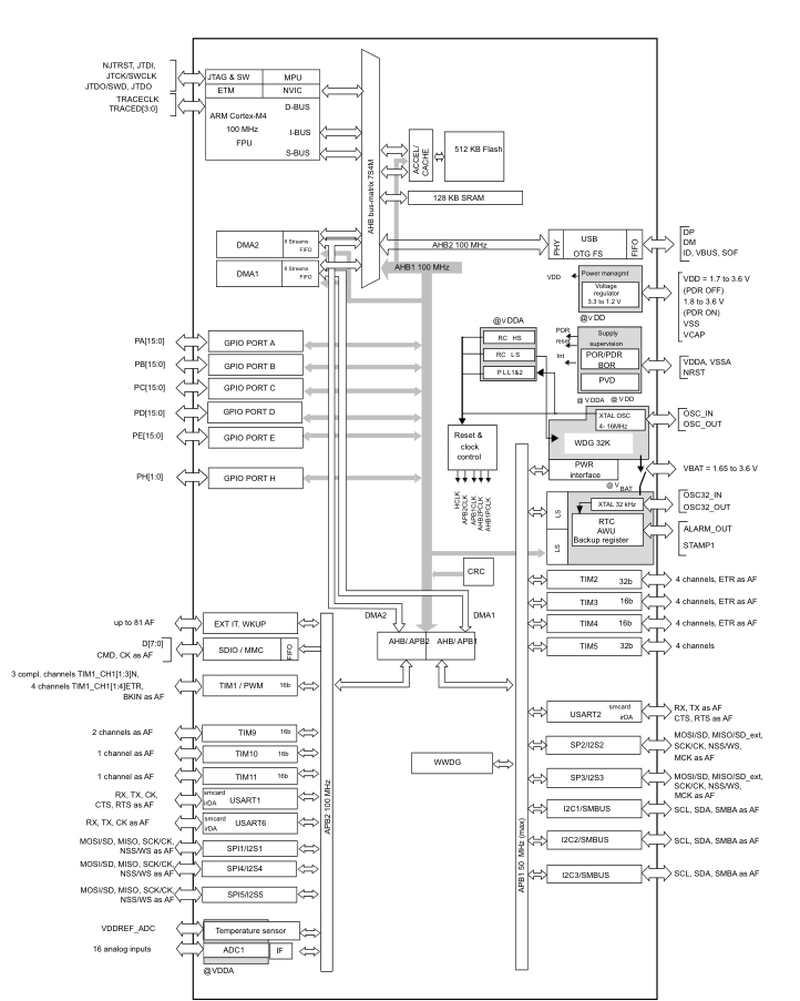
Figure 2. STM32F411xC/xE block diagram
There are various clock sources that may be used to drive the System clock via a System Clock Mux. A clock mux selects one of several inputs and propagates that signal forward to one of the AHB bus, described previously. The clock configuration chart in Figure 3 is taken from the STM32CubeIDE and is used to configure the clock system for the STM32F411RE. It's a very nice utility to learn how the clock system works but the Hardware Abstraction Layer (HAL) that's introduced when creating a project with HAL adds a lot of bulk that in most cases is not needed.
SYSCLK - The SYSCLK is the main system clock derived from either the HSI clock, HSE clock, or from the PLL clockHCLK - The clock signal for the AHB bus (AHB1 or AHB2)PCLK1 - APB1 source after the APB1 prescalerPCLK2 - APB2 source after the APB2 prescaler
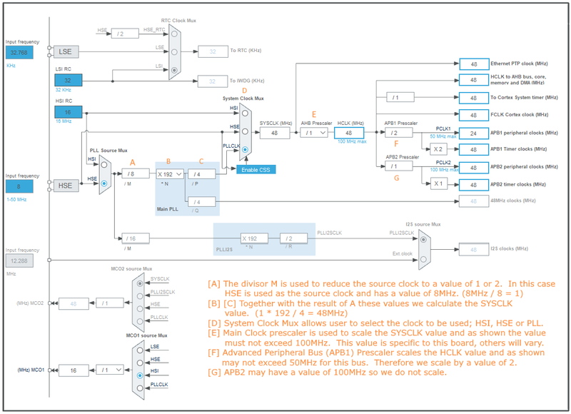
Figure 3. Clock configuration, source STM32CubeIDE
The main system clock SYSCLK can be driven by one of three sources; refer to the System Clock Mux in Figure 3:
- High Speed Internal (HSI) Clock that in the case of the
STM32F411RE is a 16MHz RC Oscillator circuit. - High Speed External (HSE) clock, the
STM32F411RE has an external 8MHz oscillator clock that is accurate and stable. - Phase Locked Loop (PLL), Variable output frequency that is processor specific, but for the
STM32F411RE processor has a maximum frequency of 100MH.
There are two more low speed clock sources that I may mention in another article. These clock sources drive the Real Time Clock (RTC) and Independent Watchdog (IWDG) sub-systems. (Refer to Figure 3.)
- LSI - 32KHz, Low speed internal clock
- LSE - 32.768KHz, Low speed external clock
Selecting the Clock Source
Setting the HSE and HSI as the system clock source is a fairly simple process and requires only a couple of steps to perform, as opposed to the PLL clock which is far more complicated because of the multiplier and various prescalers.
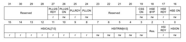
Figure 4. RCC clock control register (RCC_CR)
To set the HSE clock as system clock, set the HSEON (bit 16) in the Clock Control register. If the HSE clock source is of the type that requires a single pin, then the OSC_IN pin should be used and the HSEBYP (bit 18) set in the CR register. Once the HSERDY bit is set, indicating that the HSE oscillator is stable, the System Clock Switch bit (bit 0) in the Clock Configuration register is set to select HSE system clock source.
RCC->CR |= (1 < < 16);
while(!(RCC->CR & (1 < < 17)));
RCC->CFGR |= 0x01;
Listing 1. Programming HSE as source for SYSCLK
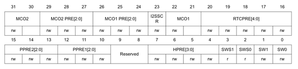
Figure 5. RCC clock configuration register (RCC_CFGR)
To set the HSI clock as the system clock, set the HSION (bit 0) and wait for the HSIRDY (bit 1) to be set indicating that the HSI oscillator is stable. Once the HSIRDY bit is set, the Switch bit (bit 0) in the Clock Configuration register is reset to select HSI as the system clock source.
RCC->CR |= 0x01;
while(!(RCC->CR & (1 < < 2)));
RCC->CFGR &= ~0x03;
Listing 2. Programming HSI as source for SYSCLK
To program the PLL as the system clock source is fairly complicated and takes some thought as to what source will drive it and the frequency that is to be output. The source to the PLL circuit can either be the HSI or HSE clocks and will need to be prescaled accordingly, as the input to the Main PLL must be equal to 1. As an example, if we set the PLL source as HSI, the M divider must be set to 16. (Refer to Figure 3 [A].)
Another factor that is critical when setting the PLL to higher frequencies is the Flash Latency wait states. Because memory is generally slower than the MPU, wait states are introduced so that the MPU will be able to communicate with memory. (Refer to Table 1.)
In the example in provided the PLL frequency is set to 48MHz, which doesn't really require wait states but was added to show how it could be accomplished.

Figure 6. RCC PLL configuration register (RCC_PLLCFGR)
RCC->CR |= (1 < < 16);
while (!(RCC->CR & (1 < < 17)))
RCC->CR &= ~(1 < < 24);
RCC->PLLCFGR |= (1 < < 22); RCC->PLLCFGR &= ~(0x1f); RCC->PLLCFGR |= (0x08); RCC->PLLCFGR &= ~(0x1FF < < 6); RCC->PLLCFGR |= (192 < < 6); RCC->PLLCFGR &= ~(0x03 < < 16); RCC->PLLCFGR |= (0x01 < < 16); RCC->PLLCFGR &= ~(0x0f < < 24); RCC->PLLCFGR |= (0x04 < < 24);
RCC->CR |= (1 < < 24);
while (!(RCC->CR & (1 < < 25)))
PWR->CR |= (0x01 < < 14);
FLASH->ACR = (1 < < 8) | (1 < < 9) | (1 < < 10) | (2 < < 0);
RCC->CFGR &= ~(0x03); RCC->CFGR |= 0x02; RCC->CFGR &= ~(0x0F < < 4); RCC->CFGR &= ~(0x07 < < 10); RCC->CFGR |= (0x04 < < 10); RCC->CFGR &= ~(0x07 < < 13);
Listing 3. PLL as source for 48MHz System Clock frequency.
The table below was copied from the Reference Manual and shows the various wait states that are required at various frequencies and power ratings. It took me a while to figure out that when I set the frequency to its maximum value that I also needed to add wait states for it to work.
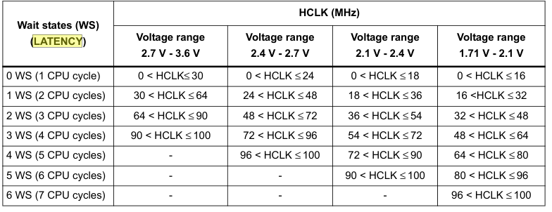
Table 1. Number of wait states according to CPU clock (HCLK) frequency
Programming the Prescalers
According to the AMBA Specification (Rev 2.0), "The AHB acts as the high-performance system backbone bus. AHB supports the efficient connection of processors, on-chip memories and off-chip external memory interfaces with low-power peripheral macrocell functions. AHB is also specified to ensure ease of use in an efficient design flow using synthesis and automated test techniques."
SYSCLK may be scaled to provide the CPU clock (HCLK) frequency by programming the AHB Prescaler. This value can be from 1-512 in powers of 2 and in the case of the STM32F411RE can have a maximum frequency of 100MHz.
The code in Listing 4 is a routine that programs the AHB Prescaler. Since this is demo code and only written as a POF and not produced for production, no error checking or validation is done.
void SetAHBPrescale(uint8_t val)
{
RCC->CFGR &= ~(0x0F < < 4);
RCC->CFGR |= ((val & 0x0f) < < 4);
}
Listing 4. Code to program the AHB Prescaler
According to the AMBA Specification (Rev 2.0), AMBA APB is optimized for minimal power consumption and reduced interface complexity to support peripheral functions. APB can be used in conjunction with either version of the system bus.
The STM32F411RE has two APB buses; a low speed APB1 and a high speed APB2 that propagate from the AHB bus through a pair of AHB-to-APB bridges. (Refer to Figure 2.) Figure 2 also shows that the two DMA channels use the APB bridges to communicate directly with the various peripherals.
The code in Listing 5 are routines that program the APB Prescalers. As can be seen, the process is fairly simple, only a set of 3 bits each needs to be set.
void SetAPB1Prescale(uint8_t val)
{
RCC->CFGR &= ~(0x07 < < 10);
RCC->CFGR |= ((val & 0x07) < < 10);
}
void SetAPB2Prescale(uint8_t val)
{
RCC->CFGR &= ~(0x07 < < 13);
RCC->CFGR |= ((val & 0x07) < < 13);
}
Listing 4. Code to program the AHB Prescaler
Outputting the Clock to a GPIO Pin
Most Microcontrollers that I have worked with provide a way to output the clock to a I/O pin and ARM is no exception. Two pins are provided to allow the programmer to output one of several clock sources to one or both of the pins provided on the chip and as a bonus, they provide a prescaler for the output. For a description of what clocks are provided for output on each pin, refer to the Reference Manual.
The example code provided in Listing 6 sets the MCO1 to output clock specified by OutType to QPIOA pin 8.
void InitClkOutput(OutType typ)
{
RCC->AHB1ENR |= 1;
GPIOA->MODER |= 0x00020000;
GPIOA->AFR[1] &= ~0x0f;
if (typ > 0)
RCC->CFGR |= (typ < < 21);
RCC->CFGR &= ~(0x07 < < 24);
}
Listing 6. Code to program MCO1 to output to PA8
Another great resource is DigiKey, they have created a series of videos on the STM32 and NUCLEO ecosystems that are perfect for beginners. I'm coming over from the Microchip world where the SAM series of processors are ARM based so it wasn't a giant leap to STMicroelectronics but it was enough that it took a little time to adjust. Starting with the first video in the series introduces the user to the IDE and creating a project using the HAL framework. Getting Started with STM32 and Nucleo Part 1: Introduction to STM32CubeIDE and Blinky – Digi-Key. I'm not a big fan of frameworks but when I started, I would configure the peripheral like I wanted it and then look at the code generated, compile and run it to see what to expect. Then I created an empty project and coded it using basic CMSIS language.
Conclusion
Being new to the ARM platform and coming from the Arduino (Atmel/MicroChip) has been a learning experience. The more research I did, the more I grew to like the ARM family of processors. Since writing this article, I have ordered various other processors such as the; Cortex-M0 STM32F030K6T6 chips, Cortex-M3 Blue Pill board, and a NUCLEO-144 Cortex-M7 board. I ordered the STM32F030K6T6 chips and created a board to mount them to attempt to solder them using a rework machine I bought a while back. It ain't pretty, but it works and with time I will get better.
Also while doing my research, I viewed a lot of videos, read a lot of articles and went through a lot of posts on various sites and have provided some of the better articles and videos in the reference section and throughout the article. I hope it helps y'all as much as it helped me.
References
- ARM architecture family wikipedia.com
- The ARM Processors: A, R, and M Categories and Their Specifics sirinsoftware.com
- NUCLEO-F411RE, digikey digikey.com
- STM32F411RE Datasheet download mouser.com
- STM32CubeIDE Integrated Development Environment for STM32, st.com
- Getting Started with STM32 and Nucleo Part 1: Introduction to STM32CubeIDE and Blinky - Digi-Key, youtube.com
- STM32CubeProg STM32CubeProgrammer software for all STM32, st.com
- STM32F411 Micro Processor, st.com
- Introduction to STM32CubeIDE st.com #60: Basics of Phase Locked Loop Circuits and Frequency Synthesis youtube.com
- ARM Product families arm.com
- stm32cube-mcu-package github.com
- LPC1768: SysTick Timer exploreembedded.com
- #7 ARM Microcontroller Tutorial - Changing the Clock to 48Mhz Using the GNU Library youtube.com
- The Advanced Microcontroller Bus Architecture: An Introduction, June 02, 2019 by Stephen St. Michael allaboutcircuits.com
History
- 6th February, 2023: Initial version
Currently enjoying retirement and working on projects without pressure, deadlines or any kind of management.


 General
  News
News  Suggestion
  Question
  Bug
Bug  Answer
  Joke
Joke  Praise
  Rant
Rant  Admin
Admin 


